Ga naar Gerards page / go to Gerards other pages ---->>> ![]()

sansui au-888 refurbishment / recap / modifications, 2019
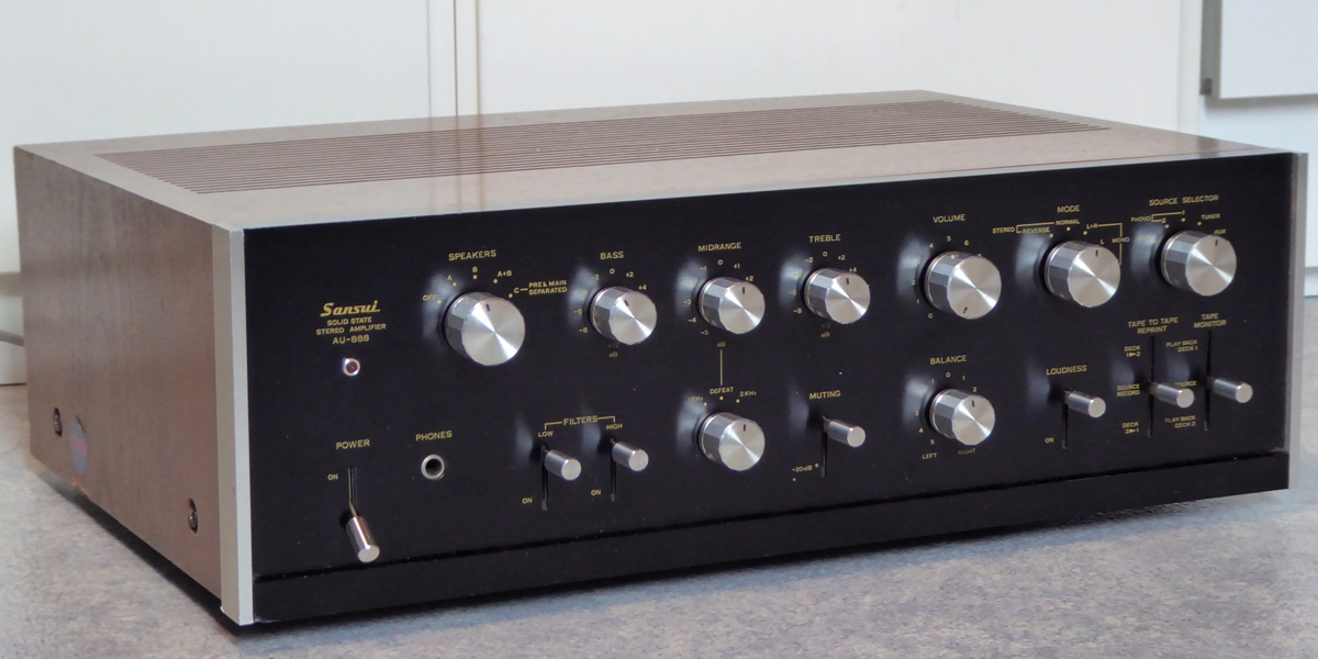
This amplifier is the one I use in the living room, it drives a pair of "Rogers Monitor" loudspeakers, a kit sold on the Dutch market. (not the Britisch Rogers)
![]() Gemakshalve is deze pagina alleen in het Engels geschreven.
Gemakshalve is deze pagina alleen in het Engels geschreven.
![]() This page is written using English language only.
This page is written using English language only.
This sansui au-888 was still in more or less working condition. It was decided to freshen it up anyway.
The power supply and protection was changed, some modifications were done, and a most electronic parts were replaced.
I did not keep a log of every part type replaced (mostly transistors and capacitors), the intention was to review the parts choices as the updating went on the fly without writing down everything.
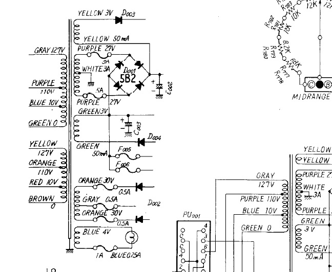
This particular unit appeared to have a nonstandard power supply layout, having some additional fuses for the "ripple filter". However, one of the schematics to be found on the internet does give specific information on this.
The circuit cards involved are mentioned one by one below, more or less in order of appearance in the service manual. The service manual and schematics can be found at several sources on the internet.
I also did put some information about the workflow to update this amp on the Audiokarma discussion forum, which can be found here. I recommend this forum as a big source of information on old Sansui amplifiers.
Component references may be of one channel only, while a second channel has an offset of 1 in the part numbering.

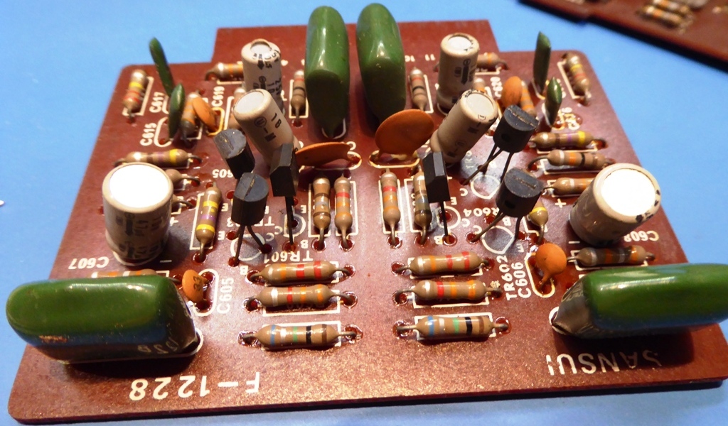
The Head Amp block F-1228
A small modification was found on the bottom of this turntable/microphone input board, which is a 100 ohms resistor in series with each output capacitor C613. I do not see it on any of the schematics of AU888 nor AU999.
However, it appears to be a factory modification as there is no indication of resoldering, which would be visible. The C615 , 6 nanofarad capacitors were a little off value, one was about 5.8 and one 6.2 nanofarads. This is acceptable deviation as per design, but not for me. Having no 6 nanofarad capacitors available as they are no standard values, 2.7 and 3.3 nanofarad ones were put in parallel, they just did fit together in the holes. The 100 ohms series resistor is put on the component side now.
Transistors change: TR601 became a 2SA970BL, TR602 a KSC1845, TR603 a KSA1015.
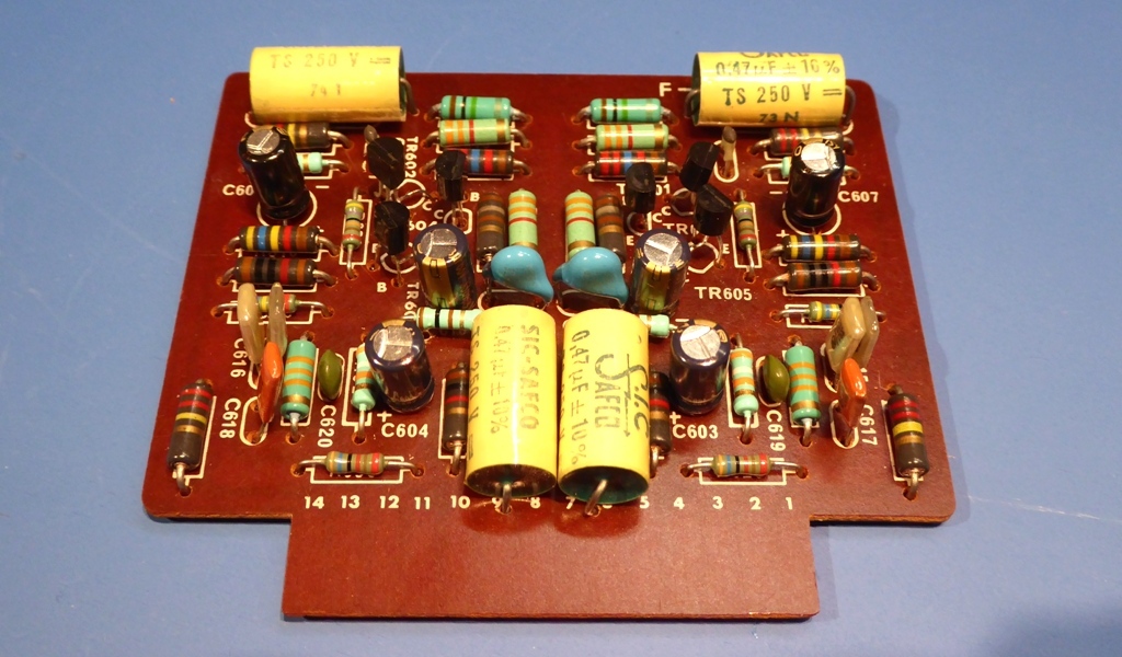
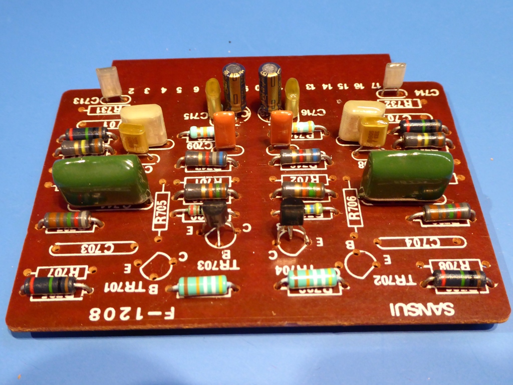
The Filter Block F-1208A
The board is supposed to be F-1208A, but actually a F1208 was found in the amplifier.
Apart from renewing the two electrolytics, there was no real reason to repopulate the board, but while cleaning the others, this was done, too.
Most capacitors were renewed as well as the resistors. Part of the NOS resistors I use are supposed to be metal films brand Corning Glassworks, I like them as they have thick tinned copper leads and element connections (they do not stick to a magnet...)
Due to the very low current I presumed a high HFE transistor was wanted so the 2SA640 found having HFE of 250 was replaced by a BC560C having HFE almost 600.
So, what is the noteworthy thing? A lot of parts LOOK missing! This is because of only the F1208A parts are mounted on the F1208 board. The "missing" ones are easily identified in the picture. All components were found as drawn in the F1208A schematic. The F1208 does exist in the Sansui AU-999
160 k resistors were added from the output capacitors (pin 8 and 11) to ground, to get rid of the lack of a ground reference to the electrolytic capacitors.
This lack of reference voltage can be regarded as a design error, as this voltage was depending on capacitor leakage and depending on which one leaks most it could reverse polarity on the less leaky one and deteriorate it...
Due to lack of a turntable at the moment, this part of the amplifier was tested using a microphone, only.
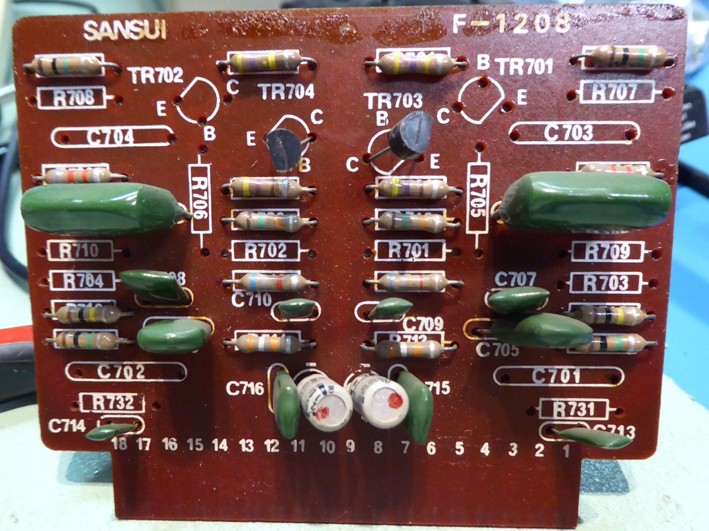
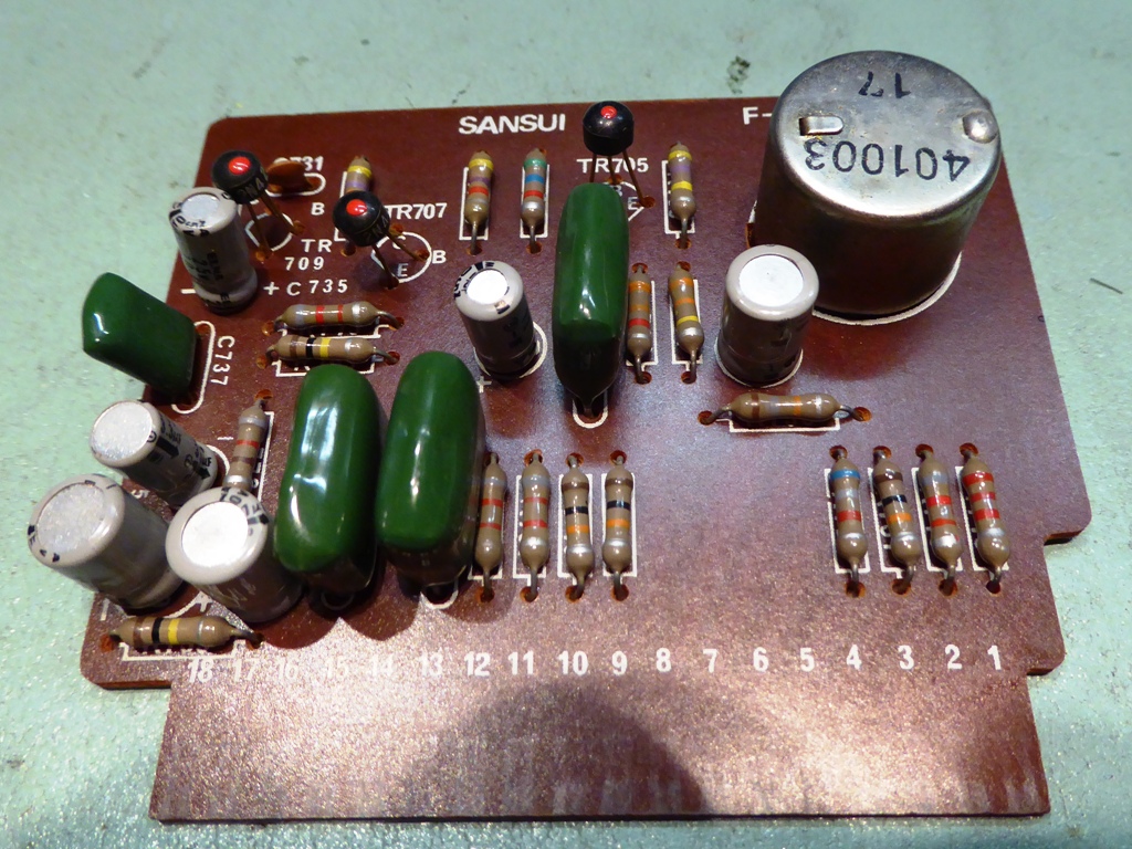
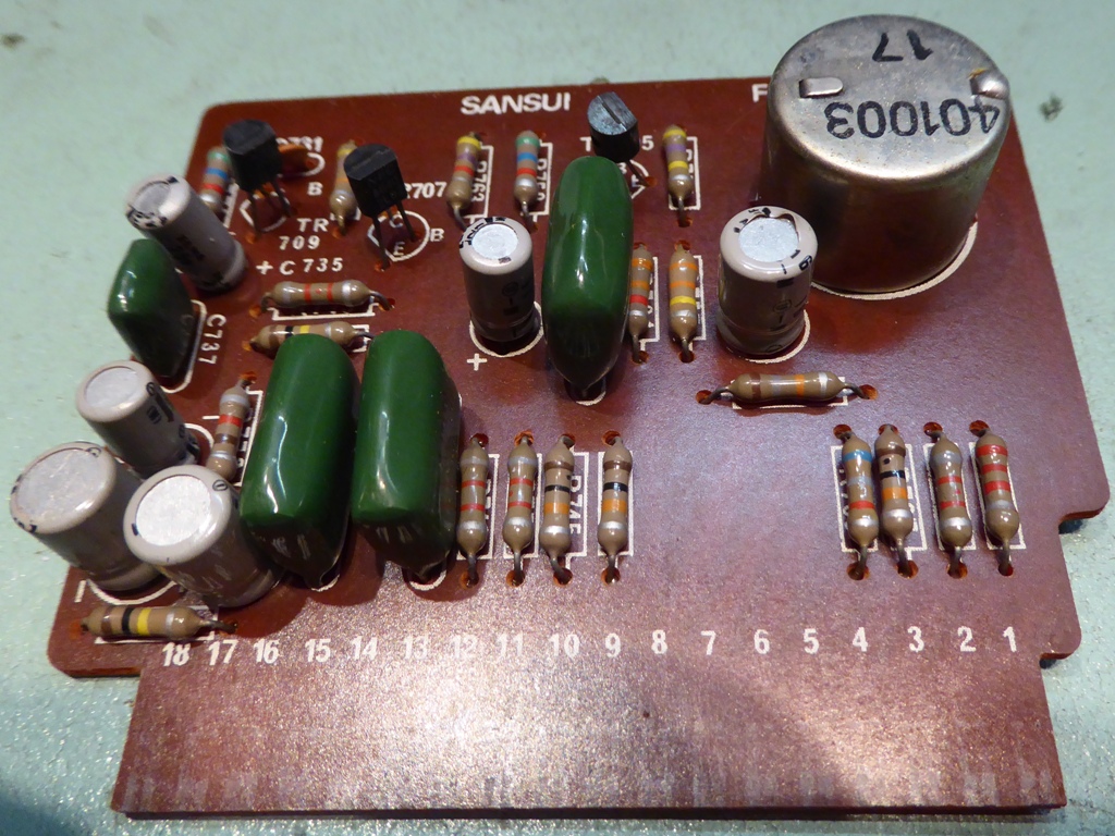
The Tone Control Block F-1209A
Also this circuit card actually is a non-A version. The F1209 Tone block board R753 is 18k. Note: it is 12k in the AU999 schematic. A modification suggested by an Audiokarma forum member was put in, to enhance maximum level swing of the NPN transistor stage.
I guessed a high HFE transistor would do in TR705 position so I put in a BC560. The other two are KSA1015.
This apart from higher value capacitors / slight resistor differences just as I desired/did and/or I did have available.
Another small difference from A999 schematicis R739 being 6.8k which is marked 8.2k on the AU999 1209 board schematic, and R747 is 10k versus something looking like 12k on the schematic of AU999.
See the AU888 and AU999 schematics for the differences, they can be found on the internet.. The position changed R755 because of the modification is easy, just mount it 90 degrees off (of course, drill a hole), as can be seen on the picture.
For the sensitivity, having R769 at 2k, I lowered R775 to 4,7k (from 8.2 k). R755 is 820k now and R759 4.7k. This circuit provides half of the previous amplification and now volume control works quite nice.One thing I did was measuring the coils which when removed from the tone boards. It is supposed to be 0.8H (according the schematic, at an undefined frequency). One measured as 0.792 which is very close (at 1 kHz) and the other 0.742 which is more off. This would lead to differences with the tone control in use.
Am I the only one checking this? (yes, I think so, in the end yu need to remove it first...).
The coils have a SET SCREW on the side. It is LOCKED by laquer on the inside, the laquer was scratched off on the one to be adjusted, the tuning of it appeared sensitive but it was succesfully done. So, this can only be done if the coil is off the circuit card, from the bottom of the coil housing.
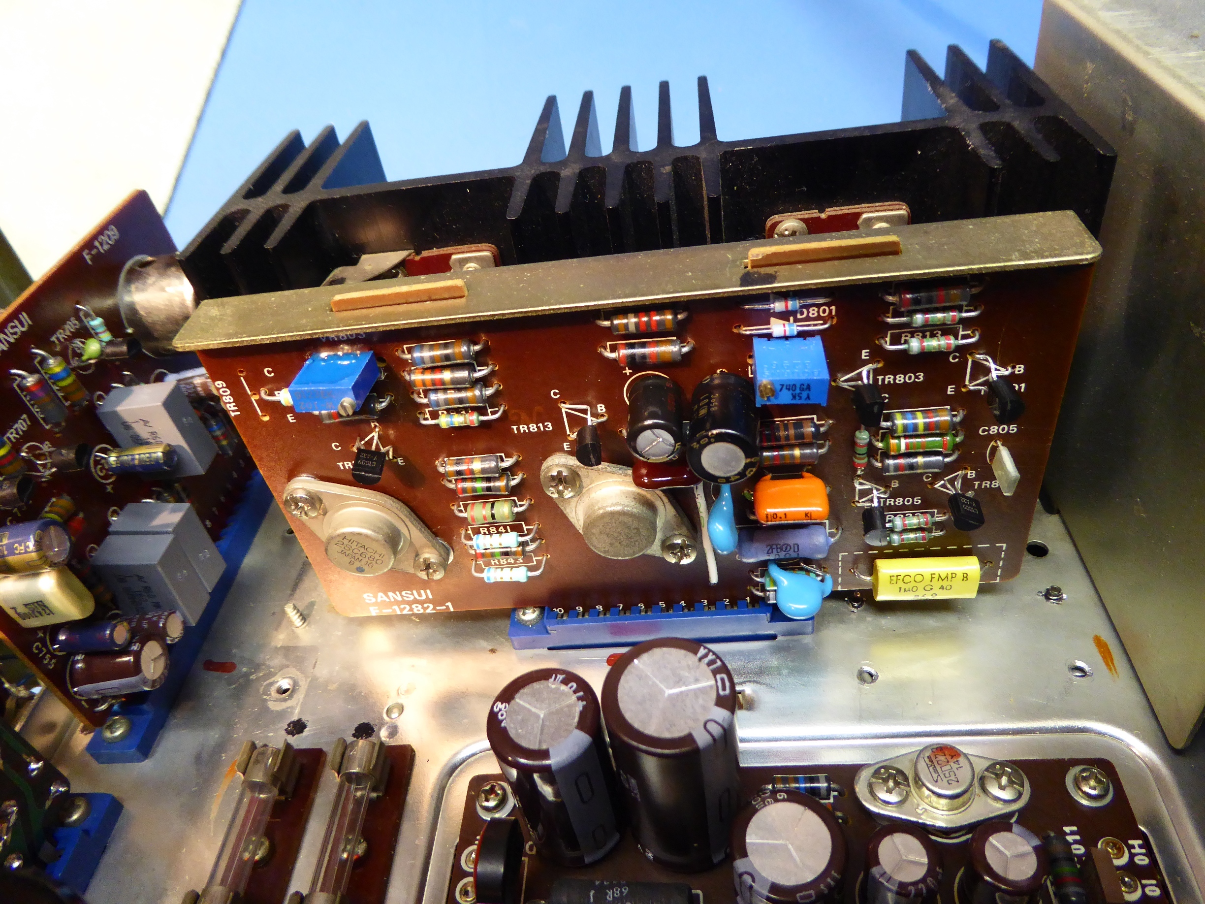
The Driver Block F-1282-1 (main amplifier cards)
As can be seen on the picture, some BC type of transistors were found on one driver card, so the amplifier was repaired, before.
The TO-66 driver output transistors, the output transistors of the amplifier, as well as the temperature sensing transistor for the bias current were retained. The other transistors were replaced as indicated in the schematic.
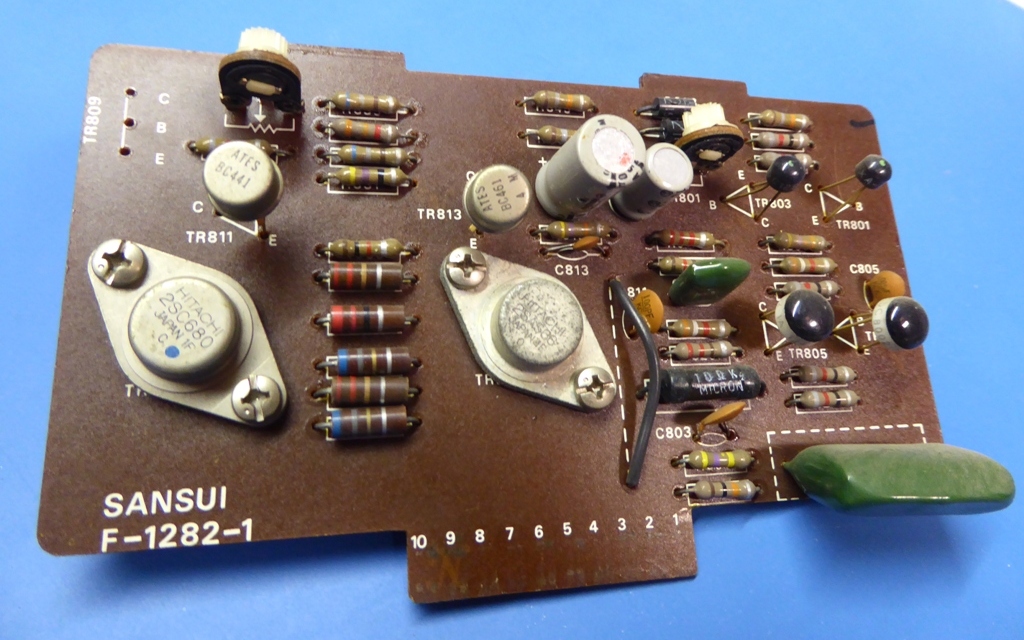
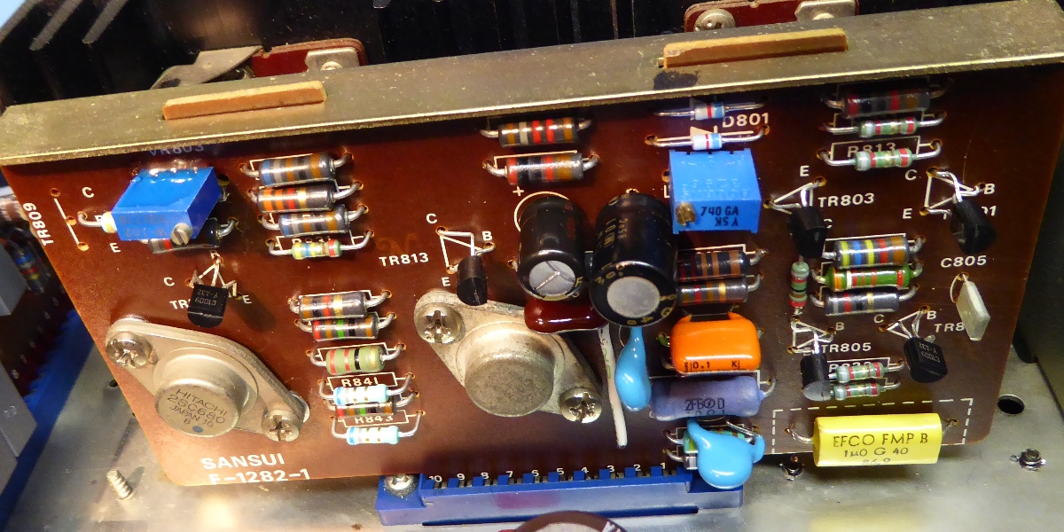
| A 820 ohms resistor was added to the tab of the DC offset potentiometer, together with a precison trimming pot the DC offset it precisely adjusted. | 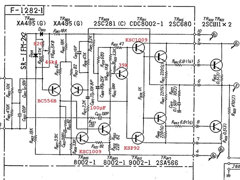 |
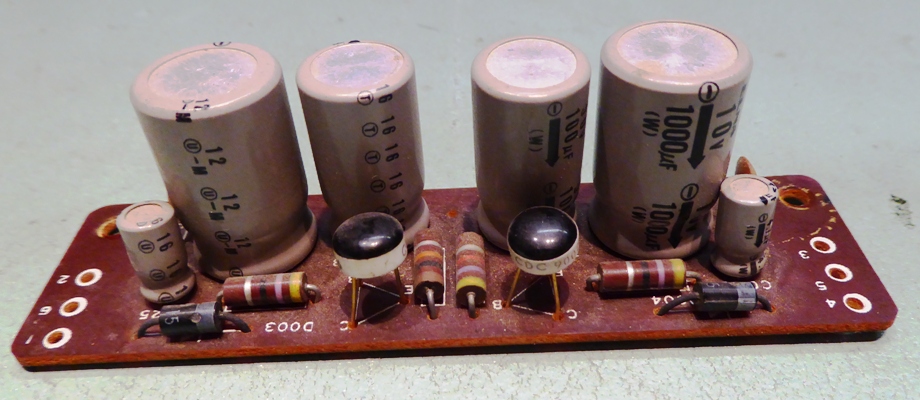
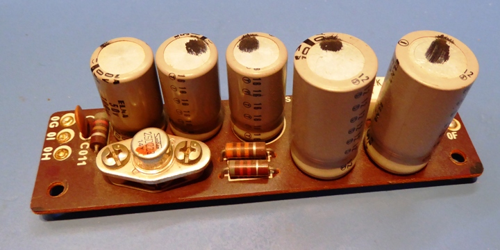
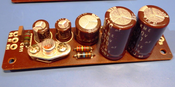
The Power Block F-1293
This circuit supplies B5 and B6, the plus and minus for the low current parts of the driver board. The circuit consists of two capacitance multiplier circuits, fed from two additional 3 Volts windings from the transformer.
Due to the low voltage and the losses through the single wave rectifiers, transistors and series resistors, the advantage of this circuit is questionable at least, since its supply is relative to the power amp plus and minus, so its supply will go up and down during high current peaks (voltage sag).
Therefore, it is somewhat modified to get the maximum out of it. To gain 0.4 Volts on each supply, 1N5820 Schottky diodes were mounted, and the output resistors were lowered to 27 ohms. I decided upping the output capacitors to 22 uF and the half wave rectifier capacitors went from 1000 to 3300 uF.
The NPN transistor became a JAN2N2219A the PNP a J2N3868. They are both more capable to withstand abuse, which can appear in this circuit in case of amp short circuit etc.(The type 9002 in the original situation suffered from low HFE, of course, the failure has a reason).
To protect the transistors, also a 1N4004 diode was mounted reverse direction from emitter to collector on each of the transistors on the bottom of the card.
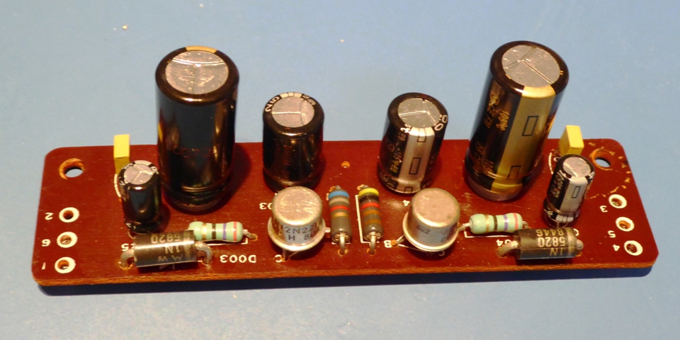
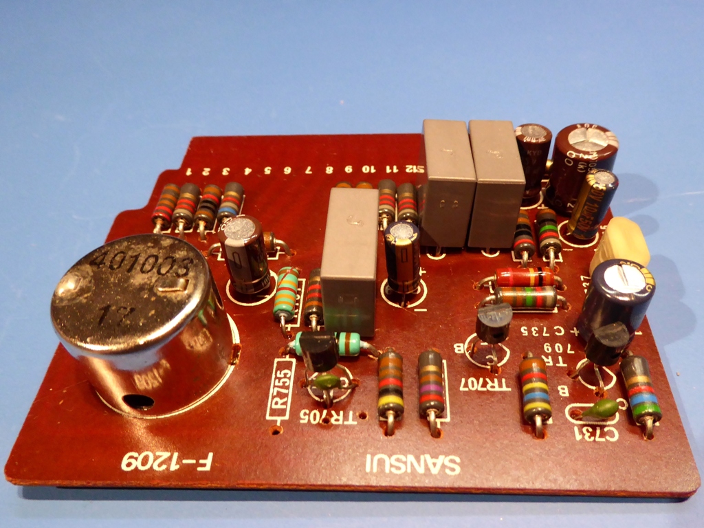
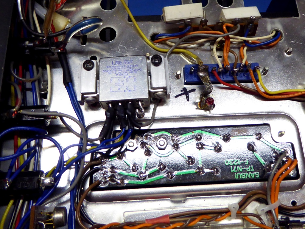
The Ripple Filter Block F-1230A
This is the stabilized B7 and B8 power source for the preamplifier boards. It has its own transformer winding, which for unknown reasons is NOT ground-referenced. This imposes some problem for implementing another user of the transformer windings as can be read later.
The F1230 is supposed to be on the AU999 according schematics but also in this AU888 it is to be found, while the schematics call for a F-1230A. Apart from the C007 on the F1230 is 220 uF and 100 on F1230A schematic there seems no difference.
All electrolytic capacitances were doubled up initially, although one of the big capacitors was made even bigger afterwards, as there was room for it. C007 went from 100 to 330 uF, just because it did fit and no other of same leg width was available.
As the old big capapacitors had signs of heating by the R003 68 ohm resistor, a bigger one was used and mounted a few millimeters above the card te enable a little more airflow.
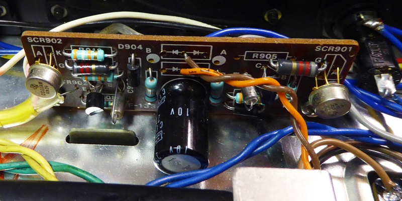
The Speakers Protector Block F-1334
This board shorts out the speakers in case of a DC level of OVER 8 Volts as tested. So, it is supposed to save the speakers but not the amplifier. The idea is the speakers fuse is supposed to blow out. In the real, the result can be damage to the amplifier itself.
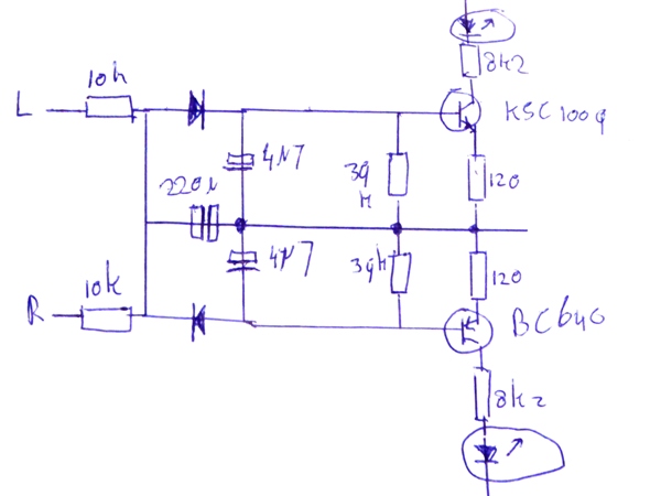
Although arguable, I decided to make a relay-type circuit protection. The speaker protection circuit is modified to be more sensitive (2.5 Volts DC), and now its use is provide an opto-isolated trigger for a newly made protection circuit. Unfortunately, I have to find back the exact schematic resembling this.
Parts were changed and two opto-couplers were used instead of the Thyristors which used to short out the circuit. Old 4N24 types were used, as they are metal-case having long leads, instead of little DIL-type opto isolators.
Unfortunately, no picture of the old protection card was made, although half of it is visible in the upper left corner of the picture below. On the right side of the same picture, part of the extra power supply fuses can be seen. On the picture of the renewed circuit, the round metal 4N24's can be seen. You can not buy those new, anymore, except for ridiculous prices at ebay.
The DC signal coming out of a faulty amplifier is not rectified and shorted anymore, so the two dual rectifiers which were present on the original board, marked as 4 diodes on the middel top of the picture, are gone. The parts on the circuit card now resemble the schematic shown, it should be noted the drawn LED's are internal to the optocouplers.
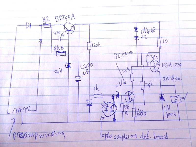
The new speaker protection circuit
The new speaker protection circuit consists of a quality relay, and a circuit card which provides a slow start of the relay if no or low DC voltage is present on the amplifier output.
In case the DC voltage rises above 2.5 Volts, the optocoupler output of the modified F-1334 board is used to open the relay again.
The relay is in series with the output fuses. As they are not needed anymore (current is also protected by the driving cards power fuses) but still having some voltage over it, they were replaced by 20 Amp fuses which have almost no loss.
At a later date, they may be removed/shorted out.
The little circuit card, as well as the relay, are both mounted on positions where small fuse assemblies were. More on those, somewhere below on this page.
The relay takes power from the low power transformer windings, so wattage offtake is minimized.
Therefore, the rectificated voltage is not directly fed to a smoothing capacitor, but topped off and fed to a big 2200 microfarad capacitor by the circuit using the BDT95 transistor, to save some marginal amount of power.
The circuit is adapted to the sensitivity of the relay.
The specific relay is way in excess of Euro/Dollar/Pound 100 new price....It is made by LRE, and certified for use in avionics, medical and military equipment.
It should be noted, this whole circuit is NOT ground-referenced due to the way the "Ripple Block" and associated transformer winding is designed by Sansui.
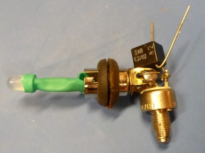
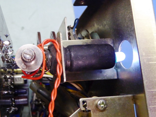
The little yellow front panel power lamp
The lamp housing was burnt more or less, it was decided to put in an adjustment potentiometer, a white LED, and a rectifier, instead.
The picture on the left was made during assembling of the piece.
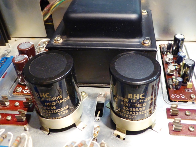
The Main Power Supply.
The two big capacitors were replaced by BHC 22000 µF 40 Volts ones, so there is about 4 times the original capacitance.
Although the originals were 50 Volts specified, even with the power supply transformer still set to 220 Volts instead of 230 or 240, the secondary DC voltage with no load never exceeds 37 Volts on the big power supply capacitors.
Average was around 35.5 Volts DC, under full 8 ohms load the voltage goes down to about 31 Volts, due to the relatively small transformer used.
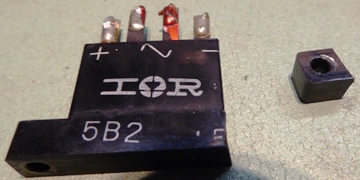
The bridge rectifier, which already physically was broken at its mounting (not affecting its operation) was replaced by a much bigger one.
As the AU888 is not a high power amp, it definately benefits from a more sturdy power supply.
Also, see the schematic part where the additional fuses are.
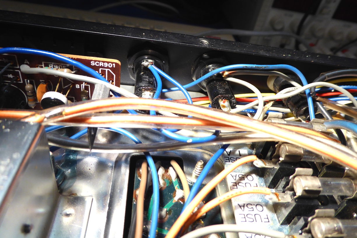
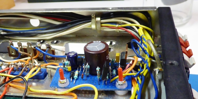
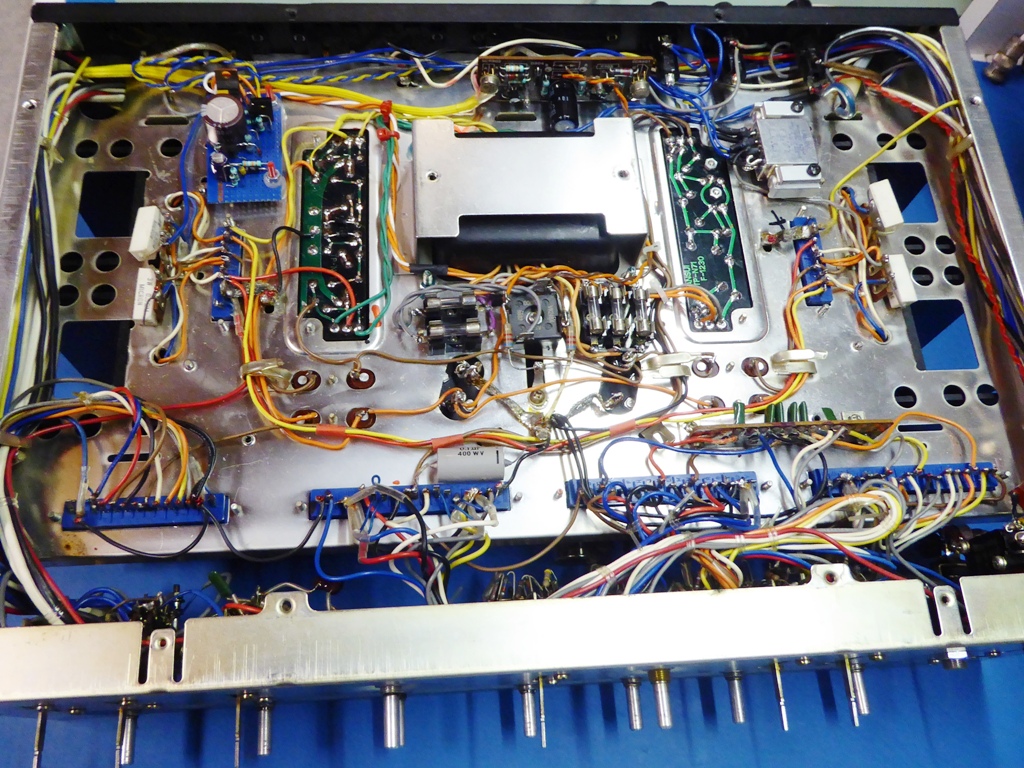
The Sansui AU888 bottom side.
On the left top of the picture, the new protect card is seen, on the right top, the protection relay.
The small power fuses, originally mounted on metal brackets, were moved to the front of the transformer, on both sides of the big rectifier, which was replaced also.
Because of some routing changes, the amount of cable mess is not more than initially, despite the mounting of extra hardware. One fuse was omitted, the one for the lamp assembly.
The Sansui AU888 top side (without metal shielding).
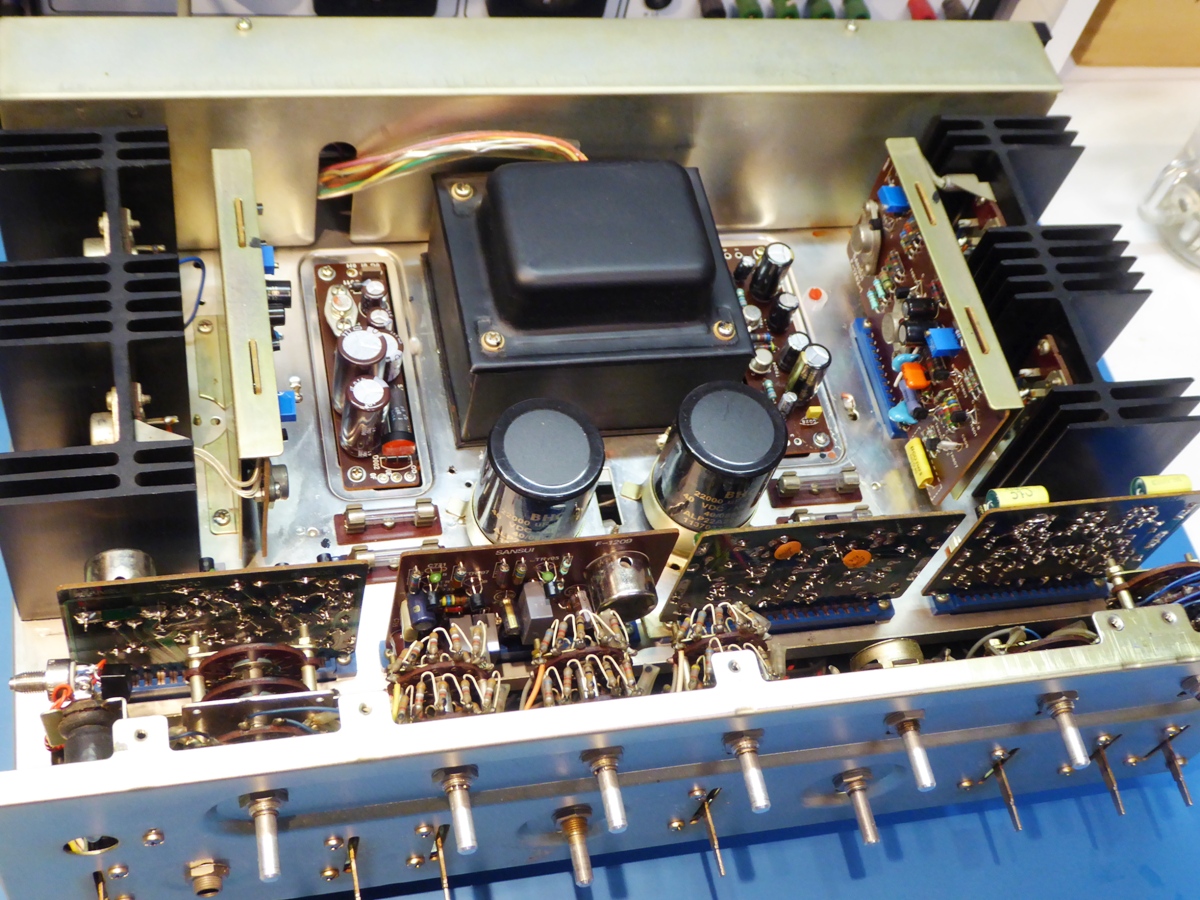
Most of the resistors used are CGW, which brand name already suggest the real glass body inside the resistors, also having thick copper wires. Good luck finding them in your local electronics shop ;-) ...
The Sansui AU888. It is in use in the living, where it drives a pair of big "Rogers Monitor MK3" TL loudspeakers, once offered by REMO as a kit and assembled by a friend.
Ga naar Gerards page / go to Gerards other pages ---->>> ![]()